Applied Physical Chemistry & Molecular Nanotechnology
Andrey TURCHANIN
Image: PrivateSince 2014, Prof. Turchanin is leading the Group of Applied Physical Chemistry and Molecular Nanotechnology at the Institute of Physical Chemistry of the Friedrich Schiller University Jena. In 2017, Prof. Turchanin was elected to the board of directors of the Center of Energy and Environmental Chemistry Jena (CEEC Jena); and since 2018 he is chairman of the Thuringia MiT-Group “2D Materials” and editor of the IOP “Journal of Physics: Materials”
The research interests of the group are focused on two-dimensional (2D) materials (graphene, carbon nanomembranes, organic monolayers, MoS2, etc.) and their hybrids for novel applications in nanoelectronics, photonics, nanosensors, energy storage and nanobiotechnology. These interdisciplinary orientation embraces (i) growth of these materials with tailored physical and chemical properties, (ii) their nanolithography, (iii) microfabrication and implementation in devices. To this end, a complementary research effort is undertaken including both fundamental and applied studies in the field of materials science, experimental physics and physical chemistry.
Research Areas
Professor Turchanin’s research interests are focused on the following topics:
- Tailored growth of 2D materials (e.g., graphene, TMDs)
- Molecular self-assembly and molecular nanosheets
- Electron irradiation induced materials synthesis
- Stimuli-responsive surfaces and interfaces
- Nanolithography and microfabrication
- Nanoelectronic and nanophotonic devices
- Chemical and biological sensors
- Energy storage and energy conversion devices
Teaching Fields
Prof. Turchanin gives courses in:
- Basic physical chemistry
- Molecular nanotechnology and nanobiotechnology
- Advanced characterization tools
- Surface science
- Nanolithography and microfabrication
Research Methods
In the Turchanin’s lab as well as in collaboration with partners the following techniques and methods are employed:
- Photoelectron and Auger spectroscopy (XPS/UPS, AES), Raman spectroscopy, polarisation modulation infrared reflection absorption spectroscopy (PM-IRRAS), second harmonic generation (SHG), surface plasmon resonance (SPR) measurements
- Scanning probe microscopy (STM/AFM), scanning/ transmission electron microscopy (SEM/TEM), helium ion microscopy (HIM), optical microscopy
- Low energy electron diffraction (LEED)
- Extreme UV interference lithography (EUV-IL), electron beam lithography (EBL), photolithography
- Electric and optoelectronic transport measurements
Recent Research Results
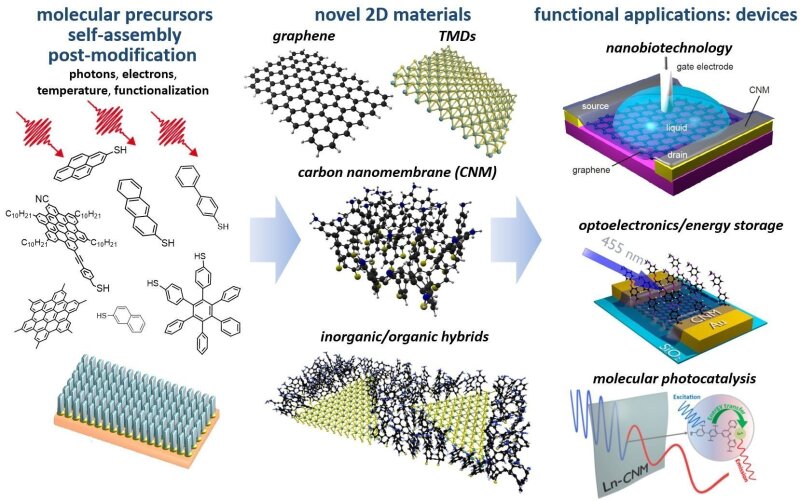
Overview on the topics and materials treated by the Turchanin research group.
Image: Andrey TurchaninAndrey Turchanin’s current research activities are focused on 2D materials (graphene, transition metal dichalcogenides, molecular nanomembranes, organic monolayers) and their hybrids with other low-dimensional materials for basic studies and novel applications in nanoelectronics, nanophotonics, nanobiotechnology, sensors as well as energy storage/ conversion, see Figure 1. These interdisciplinary activities embrace (i) tailored materials synthesis [1-2], (ii) in depth characterization by spectroscopy and microscopy methods down to the nanoscale [3-4], (iii) nanolithography and microfabrication [5-6], (iv) studying of fundamental electronic, optic and optoelectronic properties [7-8], (v) implementation of 2D materials in devices, stimuliresponsive surfaces and interfaces [9-10].
[1] Neumann et al., ACS Nano 13, 7310 (2019).
[2] Sheng et al., Small 15, 1805228 (2019).
[3] Griffin et al., ACS Nano 14, 7280 (2020).
[4] Neumann et al., ACS Appl. Mater. Interfaces 11, 31176 (2019).
[5] Winter et al., 2D Materials 6, 021002 (2019).
[6] Sırmacı et al., ACS Photonics 7, 1060 (2020).
[7] Wang et al., Angew. Chem. Int. Ed. 59, 13657 (2020).
[8] Paradeisanos et al., Nat. Commun. 11, 2391 (2020).
[9] Scherr et al., ACS Nano 14, 9972 (2020).
[10] Ngo et al., Adv. Mater. 32, 2003826 (2020).
[11] George et al., J. Phys. Mater. 2, 016001 (2019).
[12] Shree et al., 2D Mater. 7, 015011 (2020).
[13] Bucher et al., ACS Photonics 6, 1002 (2019).
[14] Löchner et al., Opt. Express 27, 35475 (2019).
[15] George et al., NPJ 2D MATER. APPL. 5, 15 (2021).
[16] Mupparapu et al., Adv. Mater. Interf. 7, 2000858 (2020).
link to the Applied Physical Chemistry & Molecular Nanotechnology Group

