Falk EILENBERGER
Image: PrivateDr. Falk EILENBERGER
Email: falk.eilenberger@uni-jena.de
Phone: +49 3641 807-274
Falk Eilenberger is the Head of Department for Micro- and Nanophotonics at the Fraunhofer Institute of Applied Optics and Precision Engineering, Jena and the Research Group Nanophotonic Materials at the Institute of Applied Physics. The research is covering fundamental and applied aspects of materials-driven nanophotonic systems. It is driven by the vision to create optical components of unprecedented functionality, by combining photonic nanostructures with innovative nanomaterials. Doing so requires and drives the understanding of light-matter interaction down to the quantum level. We do so to promote nanophotonics and to enable cutting edge applications in Science and Technology. As such, we operate a complete lithographic process chain on up to 12'' wafer scale.
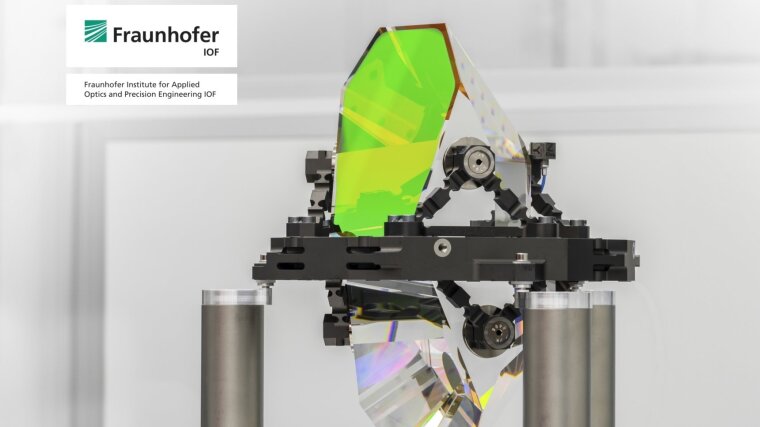
Nanostructured optical surface written by electron beam lithography.
Image: Fraunhofer IOFResearch Areas
On the materials side, we cover both active and passive materials, to be able to create and manipulate complex states of light. Modern passive optical materials for usage in functional nanostructures typically feature largely refractive indices to create dielectric metasurfaces. To be able to address the optical spectrum from the UV to the FIR we focus on materials such as TiO2 and Diamond. Active materials such as Thin Film Lithium Niobate on Insulator (LNOI) and Monolayer Transition Metal Dichalcogenides (TMDs) are investigated for their ability to create optical switches and quantum light sources on the nanoscale.
Major activities are connected by the quest to advance the design, technology, and applications of nanophotonics, by the utilizing lithographic tools in conjunction with novel materials in a creative but scalable manner. Thus, they all focus, to a certain extent, on scalable fabrication, integration in optical systems, and on the demonstration of use cases. These range from high-speed modulators for photonic and quantum systems, over highly efficient pulse compression gratings, to wafer scale computer generated holograms that enable the fabrication of the largest and most complex optical systems, such as ESA's E-ELT. We are also highly active in the development of earth observation and climate monitoring tools for space missions.
Teaching Fields
- Introduction to Quantum Communication
- Introduction to Nanooptics
- Quantum Computing
- Research Methods
Research Methods
The team and its collaborators are operating tools to experimentally realize and study optical systems embedded with 2D-Materials, among them are:
- Large-Scale Nano- and Microlithograhpic Facility: 12'' E-Beam and Photolithography tools and large assortment of etching and integration tools
- Optical characterization tools: photon-lifetime microscopy, nonlinear spectroscopy
- Nanocharacterization tools: SEM, AFM, optical near fields microscopy
- Quantum-optical characterization tools: HBT- and HOMspectrometer, high order interference experiments
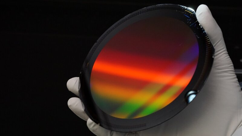
Photonic Integrated Circuits (PICs) on a wafer written be electron beam lithography.
Image: Fraunhofer IOFRecents Research Results
Recent breakthrough results in fundamental science have focussed on quantum applications of 2D-nanomaterials and their integration into optical systems, as well as algorithmic advances in quantum computers. On the application side we have shown major developments in climate monitoring devices in various missions of ESA's Copernicus programme.
We have demonstrated entangled photon sources created from so-called 2R-MoS2 [1]. This type of source is not only extremely small but also lends itself to systems integration, as has been shown in [2], where we have created highly functionalized optical fibers, which combine classical fiber optical systems with 2D-materials. We have also made advances in fundamental quantum science, showing that entanglement is a key resource in state detection [3], yielding insights into potential applications of quantum computers and future quantum sensing systems.
Metasurface devices have recently been created and delivered to ESA's Copernicus missions, which will serve to monitor the state of the atmosphere. Among these are spectroscopic devices for the direct monitoring of greenhouse gases [4] and nanophotonic devices in novel materials, in this case diamond, for the measurement of the temperature of the high atmosphere [5].
[1] Weissflog et al., Nature Commun. 15, 7600 (2024).
[2] Ngo et al., Nature Photon. 16, 769 (2022).
[3] Conlon et al., Nature Phys. 19, 351 (2023).
[4] Höing et al., Press StatementExternal link, ESA CO2m Mission (2024).
[5] Eilenberger et al., Press StatementExternal link, ESA FORUM Mission (2024).
Link to the Department for Micro- and Nanophotonics at the Fraunhofer IOF JenaExternal link
Link to the Eilenberger Group at the Institute of Applied Physics


