Carsten RONNING
Image: PrivateProf. Dr. Carsten RONNING
Email: carsten.ronning@uni-jena.de
Phone: +49 3641-9-47300
Carsten Ronning joined Friedrich Schiller University Jena in 2008 as a chair professor at the Institute of Solid State Physics. He serves as a member on the managing board of the collaborative research center CRC 1375 “NOA”, in the research council of the University Jena, as well as in the standing reviewer panel 307 of the German Research Foundation (DFG), where he has been reelected in 2020.
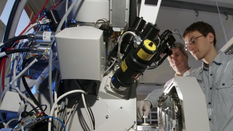
The research group is specialized in the synthesis, modification and characterization of functional, nano-scaled materials, with a strong focus on their optical and electronic properties. This includes the use of semiconductor nanowires as small and active laser devices, metasurfaces for flat optics, as well as poly-crystalline CIGS thin film materials for photovoltaics. Commonly, ion beam based techniques, e.g. such as ion implantation, are used within the group in order to induce an added or optimized functionality to the different material classes. Thus, the group runs several large scale-facilities and has a high expertise in ion-nanostructure-interactions.
Research Areas
Carsten Ronning’s research interests address nano-scale solids, photovoltaics, ion-solid-interactions, metasurfaces, as well as light-matter-interactions. Research thrusts include:
- Semiconductor nanowires: synthesis, functionalization, manipulation, optical characterization as well as lasing properties
- Photovoltaics: characterization of Cu(In,Ga)(Se,S)- and Kersterite solar cells using synchrotron und electron beam methods
- Ion solid interactions: ion beam modification of materials, effects by nanostructures, Monte Carlo simulations
- Metasurfaces: masked or focused ion beam irradiation, ion beam irradiation of phase change materials, oxides or silicon
- X-ray nanoanalysis: of functional nanomaterials and solar cells at the synchrotron ESRF in Grenoble, France
Teaching Fields
Carsten Ronning covers the full curriculum of experimental physics, which includes mechanics, optics, nuclear physics, solid-state physics, atomic physics, etc. Furthermore, he offers specialized courses on nuclear solid-state physics as well as nanomaterials and nanotechnology.
Research Methods
The laboratories lead by Carsten Ronning offer a wide range of methods for the synthesis, modification and characterization of materials.
- Ion beam doping, modification of solids and deposition, magnetron sputtering of thin films
- Structural characterization by high-resolution electron beam and X-ray methods, as well as ion beam analysis techniques
- Optical characterization of semiconductors using divers luminescence techniques
- Advanced electrical characterization, e.g. of solar cells
Recent Research Results
Metasurfaces are artificially structured and optical thin layers that can be precisely constructed to manipulate the amplitude, polarization, or phase of light. Metasurfaces thus enable flat optics and will revolutionize photonics, as conventional lithography and processes such as ion implantation can be used to fabricate complex optical devices. We realized metasurfaces by either selectively irradiating or doping materials with ions through masks. Alternatively, we introduced doping elements or defects using a focused ion beam and thus write the metasurfaces „directly“ into the material. [1, 2]
We also produce, conduct, and investigate the properties of semiconductor light-conducting wires. [3, 4] The tiny wires, which are only about ten to five hundred nanometers in diameter, are so thin that the wavelengths of visible light optimally fit in them. Perfect light guide, then. In addition, three other features make the wires remarkable: they are an „active medium“ that can emit photons, they can be pumped, and reflect the light at their ends, thus acting as a resonator. These properties make them tiny lasers. In order to exploit the full potential of such small lasers, it is especially important to find out how and how fast the laser light is emitted. We have succeeded in investigating both: for very thin wires, the light is emitted as a Gaussian beam, while the HE11 mode is dominant within the wire. This also leads to fast emissions in the range of a few ps. However, if the wires are thicker, this changes quite considerably: then the wires radiate more strongly at the edges and less at the center, and are also much slower.
Finally, our goal is to also understand the transport and recombination mechanisms of charge carriers in polycrystalline thinfilm solar cells - such as e.g. Cu(In, Ga)Se2 (CIGS) solar cells. With such findings, the efficiency can be increased in cooperation with our industrial partners and a process window optimal for the industry will be found. Today it is well known that alkali elements can lead to a significant increase in the efficiency of CIGS solar cells, but their role is largely unknown. Therefore, we extensively investigate thin film solar cells and sublayers using high-resolution synchrotron and electron beam based methods in a combinatorial approach and revealed the beneficial effects of alkali decorated grain boundaries. [5, 6]
[1] Rensberg et al., Nano Letters 16, 1050 (2016).
[2] Hafermann et al., ACS Photonics 5, 5103 (2018).
[3] Röder et al., phys. stat. sol. (b) 256, 1800604 (2019).
[4] Zapf et al., Adv. Opt. Mater. 7, 1900504 (2019).
[5] Schöppe et al., Nano Energy 71, 104622 (2020).
[6] Ritzer et al., ACS Appl. Energy Mater. 3, 558 (2020).
